POL is a power semiconductor specific package technique by which electrode connection and wiring are performed by using printed circuit board manufacturing technology. POL assures high precision and stable shape reproducibility. The low conduction resistance and high-speed switching performance of not only Si power semiconductors but also new material power semiconductors such as SiC and GaN can be maximized.
Features
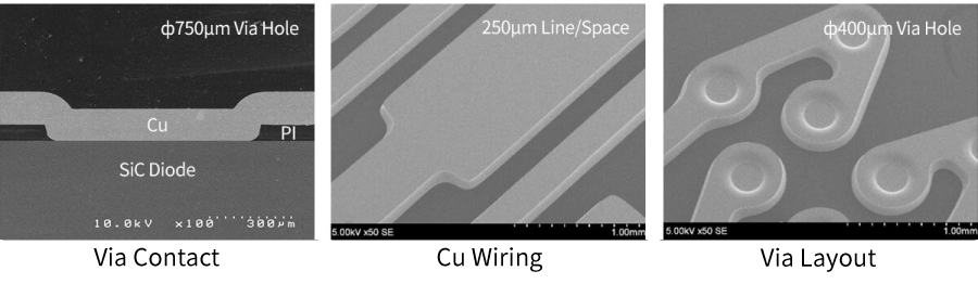
High dimensional precision and stable shape reproducibility of power circuit connection and wiring are provided by the pholithography technology of substrate manufacturing process
High reliability is achieved by direct copper joints (plated metal connection) of die to substrate patterning
Power device specific materials (i.e., thick copper plating, substrate materials, and adhesives) applied to high voltage, large current and high heat dissipation devices
Development of the power supply units with low conduction loss, low switching loss, short switching dead time and high heat dissipation
Achieve small form factor, lightweight, high efficiency and long lifetime for power system
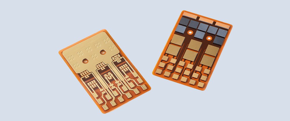
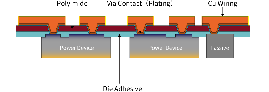
Structure
Applications
Inverters, converters, switches, etc., for drive motors in aircrafts and large industrial equipment
Inverters and converters for xEV drive motors
Inverters, converters, switches, etc., for power conversion equipment in energy generation and storage
Custom design switching power supply units (electromechanical devices, etc.)