We develop and produce of various “Semiconductor Packages” adapting for the miniaturization, acceleration, and performance enhancement of semiconductors.
We aim to enrich and contribute to the lives of people all over the world through providing our cutting-edge packaging technologies, including for markets related to IoT and AI, which are anticipated to become more widely used in the future, and auto market, in which technology development is accelerating, such as autonomous driving and electrical vehicles, supported by the practical implementation of the next-generation mobile communication standard (5G).
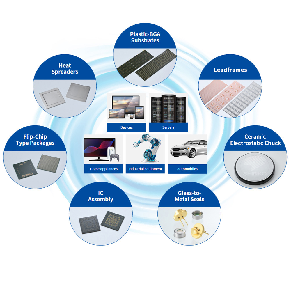
Our Products
We provide products and services that meet the needs of the market, with the central focus being semiconductor packages based on a variety of elemental technologies we have accumulated since the founding of our company.
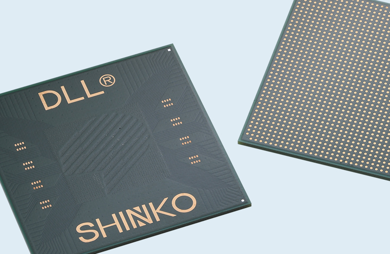
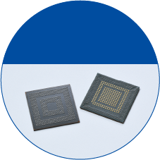
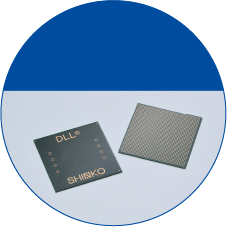
Flip-Chip Type Packages
Also called build-up substrates or flip-chip packages, they mainly see use in advanced IC chips such as CPUs for computers and servers. These packages meet the need for high-speed and high-density semiconductors through fine wiring patterns, multilayered structures, and superior electrical characteristics.
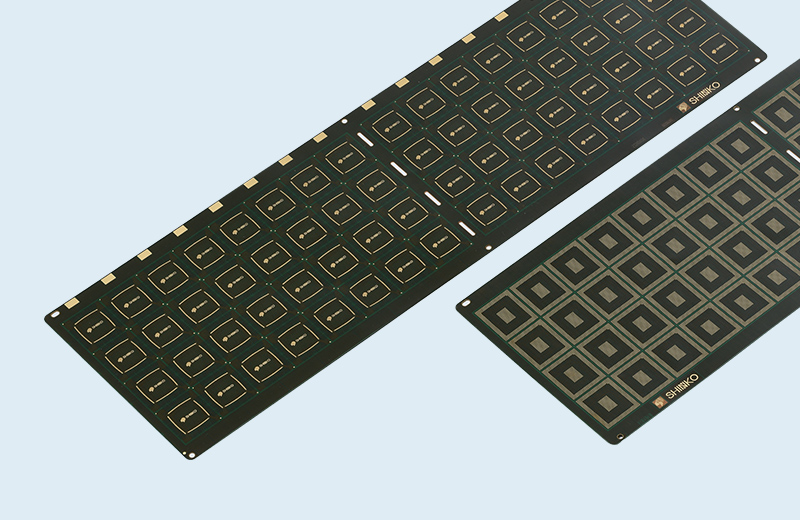
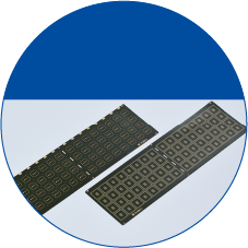
Plastic-BGA Substrates
These substrates are mainly used in memories, controllers, and automotive applications. Fine wiring patterns and multilayer structures support the miniaturization, densifying, and thinning of semiconductors.
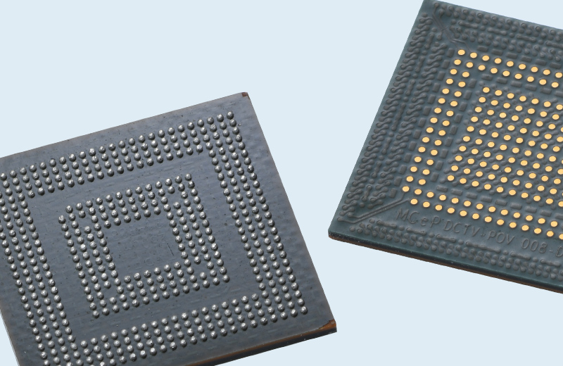
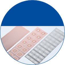
IC Assembly
We perform IC assembly (packaging) for mounting IC chips in packages. We meet the needs of our customers through advanced internal connection technology compatible with a variety of packaging types.
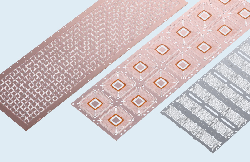
Leadframes
Our Leadframes are manufactured with stamping technologies using extraordinarily precise dies and various plating technologies. These Leadframes see use in wide range of applications, such as in smartphones, PCs, automotive and consumer electronics, and more. We produce not only stamping Leadframes but also etching lead frames to meet a variety of needs.
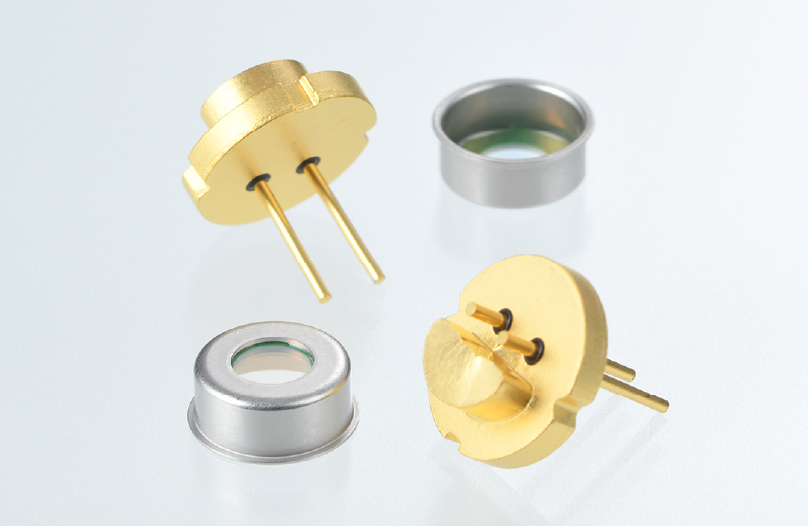
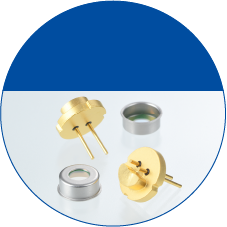
Glass-to-Metal Seals
Glass-to-metal seals are mainly used for laser diodes and sensors for in-car use. Its high hermeticity and superior electrical characteristics meets the needs of fields that demand a high degree of reliability.
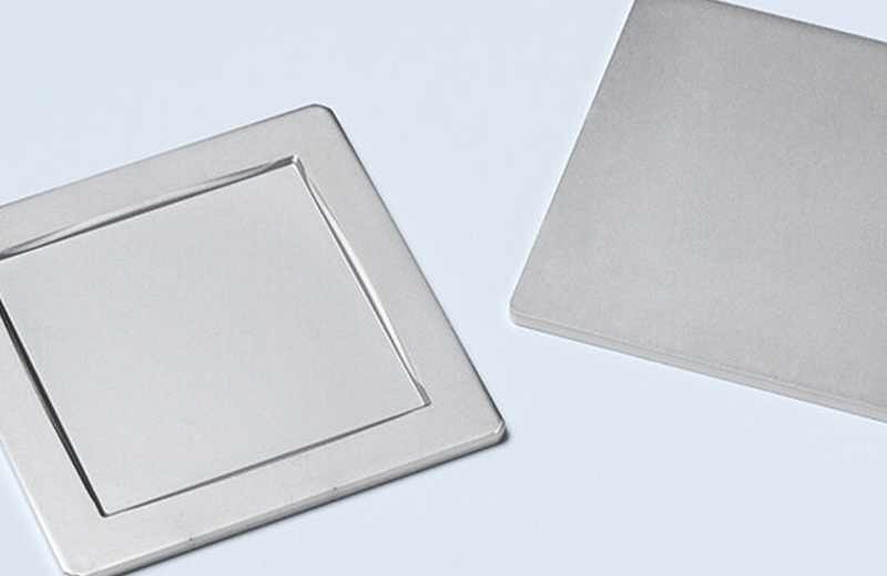
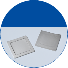
Heat Spreaders
Used in CPUs found in PCs and servers. Through excellent stamping process and plating technologies, heat generated by IC chips is efficiently and quickly dispersed, ensuring stable operation and function.
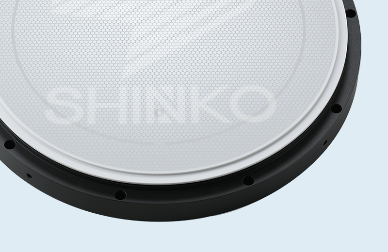
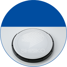
Ceramic Electrostatic Chuck
Ceramic electrostatic chuck sees use in etching machines for semiconductor manufacturing equipment. We respond to the advanced needs of our customers through ceramic manufacturing technology we have cultivated over the years.
Electronic products, such as PCs, smartphones, and other home electronics with various functions that incorporate advanced semiconductors, are used for people’s abundant lives and have become indispensable to our society. Semiconductors are expected to greatly spread the usage continuously as a key technology such as in automobiles, in which technological development is accelerating, including with autonomous driving and EV (electric vehicles), and applications related to the IoT and AI, which is envisioned to expand rapidly in the future.The semiconductor market is anticipated to keep glowing.
With our wide range of products and various technologies, we cover the entire semiconductor packaging area to become unparalleled in this industry, and we provide our products and services to a variety of markets.
Please click each product icon and see the application of our products.
We have regarded “Technological Development” as one of the most important guidelines of our management since our foundation, and have focused on the development and the accumulation of new technologies. Technologies acquired and developed in this way form our core technologies.
As new needs arise, we will continue to strive to meet them, developing and deepening our core technologies to transcend the times and bring the exceptional functions of semiconductors into people’s lives.
Please click each technology icon and see our technology details.
Hermetic Sealing Technology
This technology has been used since our company was founded, first applied to recycling household lightbulbs. Technology that joins metal, glass, and more while maintaining air tightness is used in products that require a high degree of hermetic sealing and resistance to high temperatures.
Ceramic Processing Technology
This technology turns ceramic powder into a paste and hardens it into a variety of shapes. Metal pattern wiring and drilling on ceramics are available at our company. While this technology was used for manufacturing semiconductor packages, at present, they are also used for manufacturing the core parts (ceramic electrostatic chucks) of semiconductor manufacturing equipment.
Multi-Layering Technology
This technology is used to produce substrates with multilayer wiring. With our fine-wiring forming technology and mass-production capacity, we support the evolution of advanced semiconductors.
IC Assembly Technology
Our technology assembles various types of semiconductor devices. We have the technology for wafer thinning, electrically connecting IC chips to substrates, and molding with dedicated material to protect the IC chips from external environment.
Photolithography and Etching Technology
Photolithography is a fine-wiring forming technology based on photographic development technology. Etching is a metal melting technology using corrosive action of chemical agents. With this high-precision technology, we can form electric circuits thinner than the width of a human hair.
Organic Material Processing Technology
We have the technology for processing plastic materials mechanically, chemically, physically, and thermally. This is an important technology for making semiconductor packages smaller, thinner, and lightweight.
High-precision Plating Technology
Our high-precision plating technology applies to various materials used in semiconductor packages. The resulting materials gain characteristics required for semiconductor packages, such as electrical connectivity and corrosion resistance properties.
Die Making and Precision Machining Technology
We have the technology for stamping and drawing materials with high precision, and use it to produce various types of dies and precision parts.