Introduction
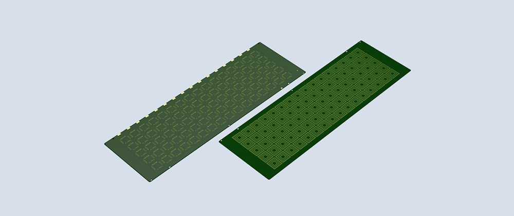
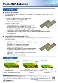
SHINKO supplies organic substrates using prepreg for BGA packages for logic, memory, and sensor devices. 2 layers or 4 layers through-hole substrates are used for devices such as automotive application requiring high reliability. Build-up substrates that can use multi-layer structure are used for semi-conductor packages that require size reduction and high density.
Features
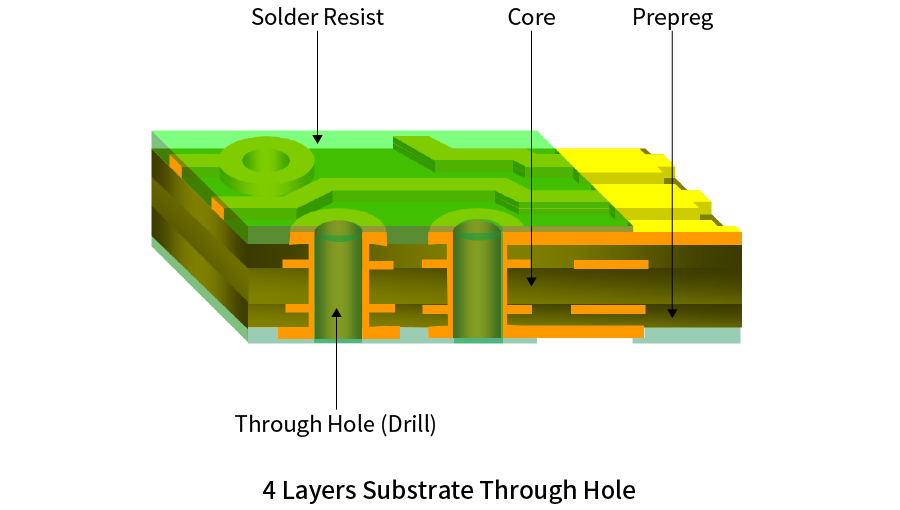
2 Layers/ 4 Layers Through Hole Substrate
- Substrate with low cost and high reliability
- Superior electrical characteristics
- Etch back process is supported
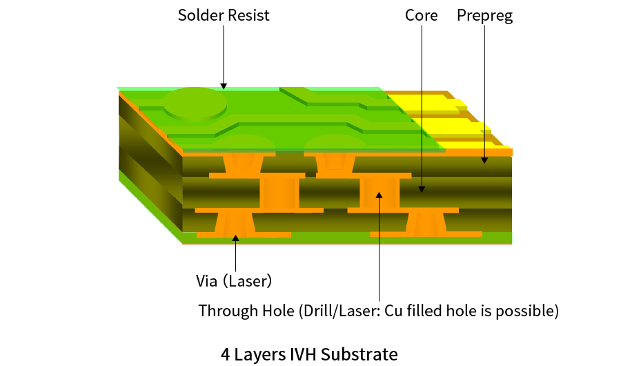
Build-up substrate (IVH* substrate)
- Superior electrical characteristics
- High density is possible by using semi-additive process and laser vias
- Multilayer structure consisting of 4 or more layers is possible
- Structure of via on PTH (Plated Through Hole) and structure of stacked via are supported
- Thinner substrate thickness is available by using thin core
- Etch back process is supported
- Available for both WB (Wire Bonding) and FC (Flip-Chip)
*IVH: Interstitial Via Hole
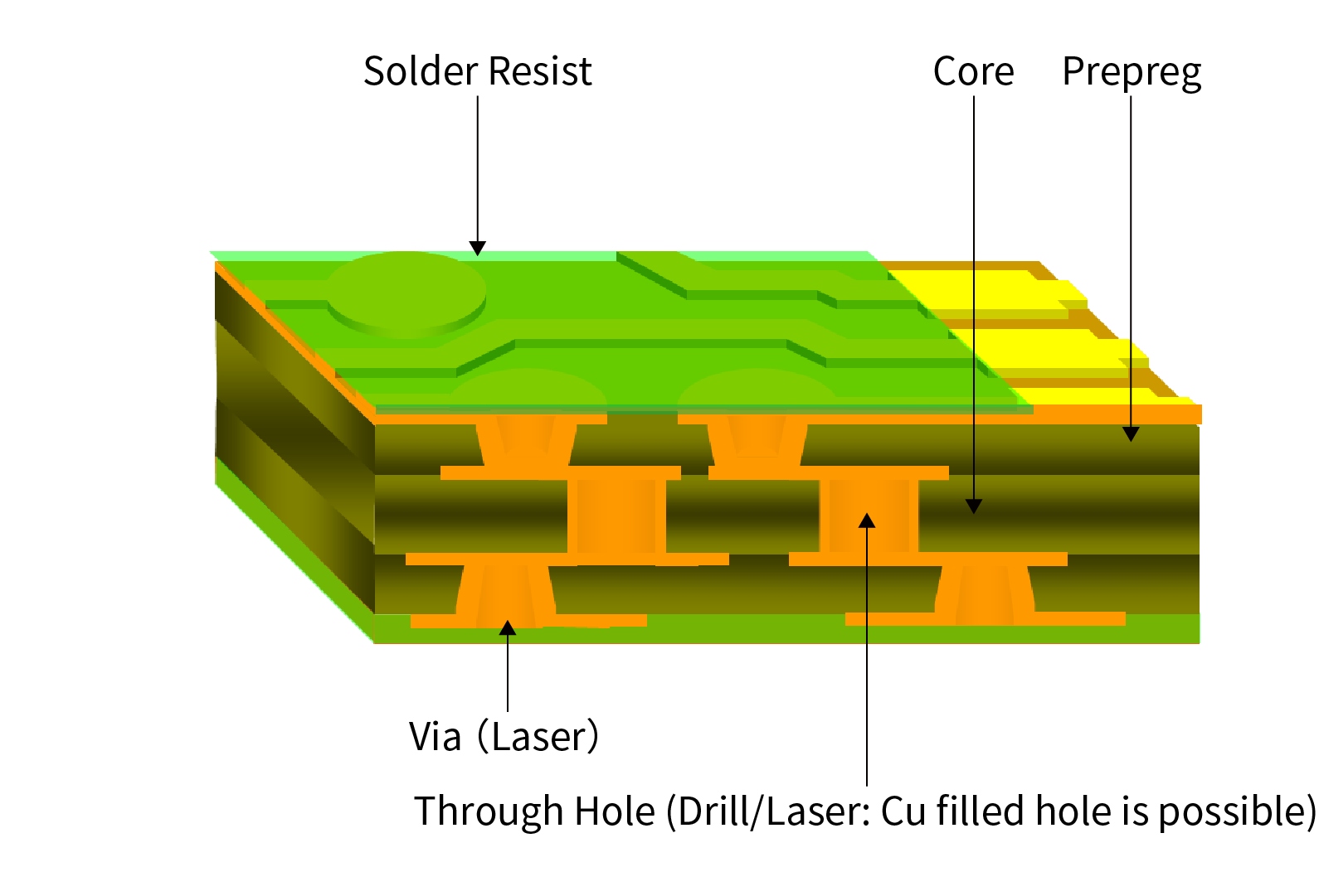
Structure
Applications
- Chip sets
- Controllers
- Memory
- ASIC
- Image sensors
- Devices such as automotive requiring high reliability
Technical Document (Download)
Substrate
PBGA Substrate
Click on download the PDF file and view details.


