SHINKO ELECTRIC INDUSTRIES CO., LTD.
SHINKO ELECTRIC INDUSTRIES CO., LTD.
As copper has superior properties as electrical wiring material, the electrolytic copper plating method produces wiring patterns with lower cost compared to other film formation methods. The via fill electrolytic copper plating method for printed circuit boards has been improved over the last 20 years. As a result, many types of additives are available at present, and they can be selected and used according to customers' use purposes.
However, deeper blind via holes and finer wiring must be made for developing substrates with new structure for semiconductor packaging as conventional plating solution may not perform sufficiently in some situations.
By optimizing all plating processes in the chemical, electrical, and mechanical fields, SHINKO maximizes plating solution capacity and applies it to new products.
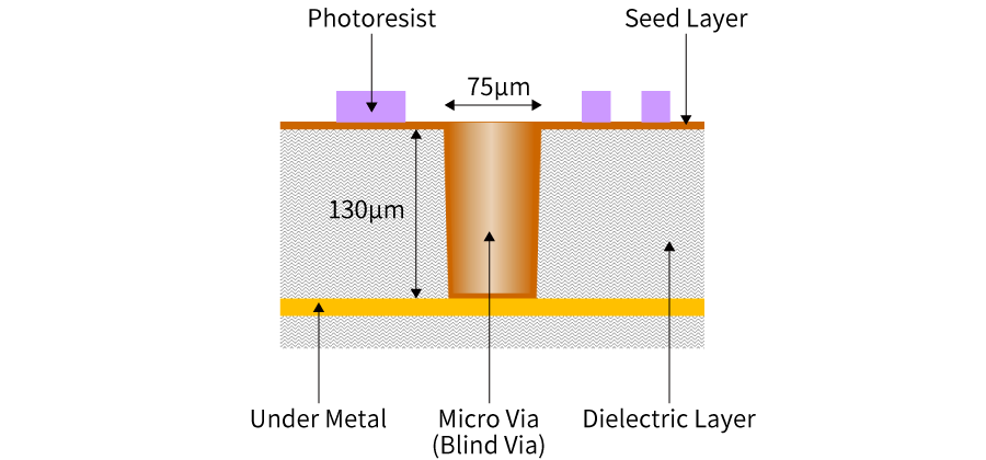
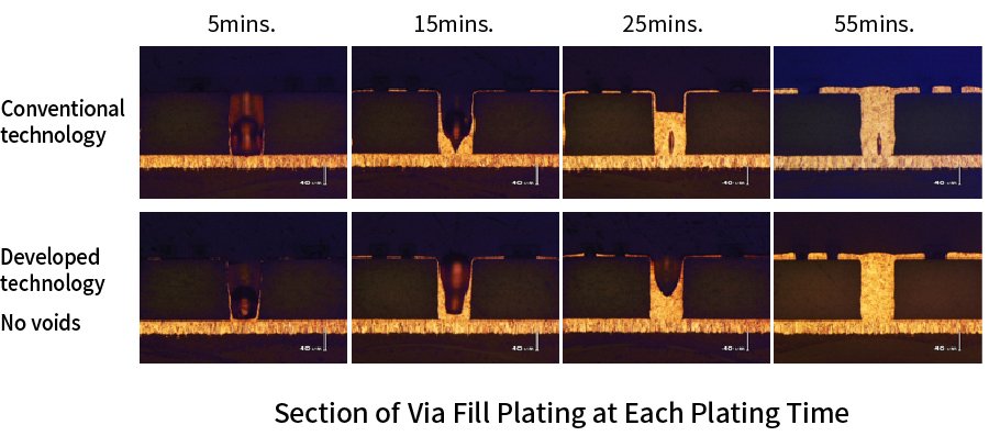
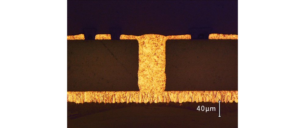
When electrolytic copper plating technology for new structure package substrates with high-aspect-ratio deep blind via holes is used, no-void filling cannot be performed by adjusting plating solution basic composition or additive concentration. When the cross section of vias during plating was observed, it was found that voids were formed near the bottom in the first half of the plating. This means that accelerator on the side wall of the via bottom works too hard. To suppress the effect of the accelerator, reverse electrolytic pulse plating technology was applied. As a result, no-void filling was achieved.
Generally, it is said that reverse electrolytic pulse plating technology is difficult in condition setting and mass production. However, SHINKO solves such problems with our unique know-how.

