SHINKO ELECTRIC INDUSTRIES CO., LTD.
SHINKO ELECTRIC INDUSTRIES CO., LTD.
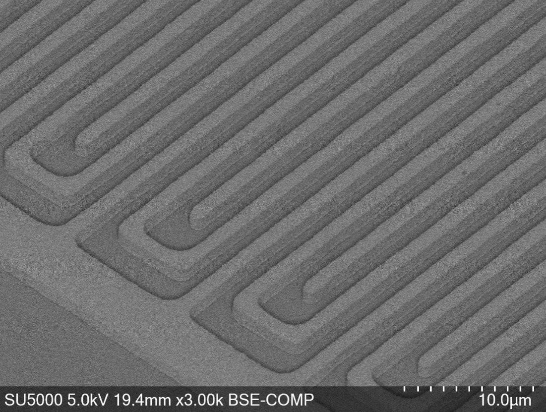
As electronic devices have acquired higher performance and higher processing speed, heterogeneous structure (in which different types of IC chips are mounted in one package, represented by Si interposers and fan-out packages) has been developed. SHINKO developed fine wiring and photo-vias technologies for fine pitch substrates and organic interposers by using plasma technology, sputtering technology, and photolithographic technology.
State-of-the-art copper fine wiring and photo-vias using photosensitive insulating resin can be formed on a substrate by combining the semiconductor package substrate manufacturing process with the technology used during the IC chip manufacturing process.
Sputtering films were introduced on semiconductor package substrates in lieu of electroless plating seed layers, and plasma processing was introduced for hydrophilizing before electrolytic copper plating. After the patterning resist of electroless copper plating is removed, a fine line width of 1.5 μm can be achieved by introducing the cleaning plasma ashing process.