SHINKO ELECTRIC INDUSTRIES CO., LTD.
SHINKO ELECTRIC INDUSTRIES CO., LTD.
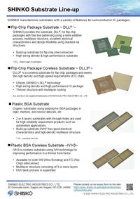
Substrate
* DLL (Direct Laser & Lamination).
DLL and DLL3 are registered trademarks of SHINKO ELECTRIC INDUSTRIES CO., LTD.
Due to the recent performance improvement of IC chips in electronic devices such as PCs, servers, etc., the demand for flip-chip package substrate using build-up process has been increasing due to providing the benefits of higher speed and higher density.
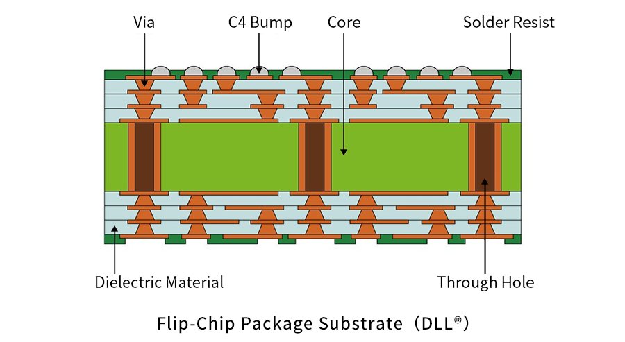
SHINKO provides flip-chip package substrates, DLL®, which have the fine line patterning through the use of a semi additive process, multilayer structure, and excellent electrical characteristics and design flexibility through the use of stacked via structures.
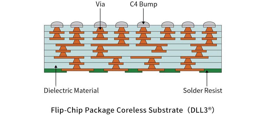
Also, to meet the acceleration of high-density and high-speed of IC chips, the demand for flip-chip package substrates with high density, good electrical performance, and a thinner structure has been increasing. Therefore, SHINKO has developed the coreless package (DLL3®) which has thinner thickness structure coupled with good electrical performance and high design flexibility.
Used in devices requiring high-density routing
Click on download the PDF file and view details.