SHINKO ELECTRIC INDUSTRIES CO., LTD.
Contact Us
Search by Product Name
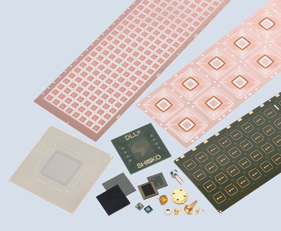
Semiconductor Package
Thermal Management Parts
Product for Semiconductor Manufacturing Equipment
Metal Products
Search by Application
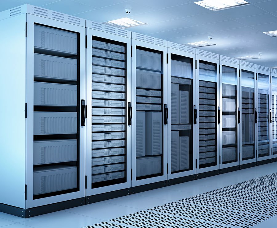
Computing & Networking
Mobile
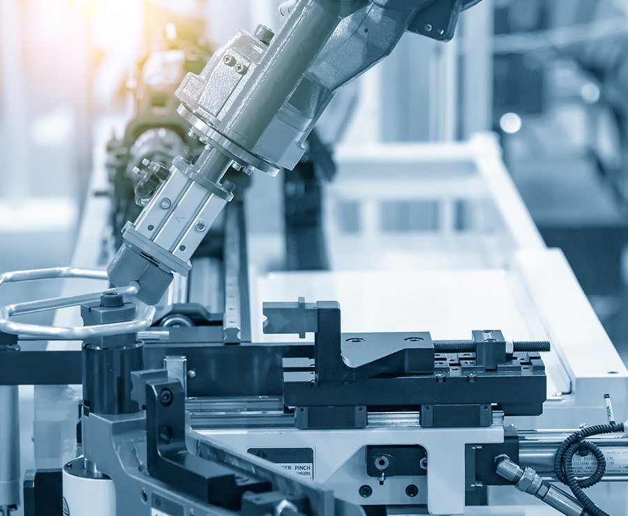
Industrial & IoT
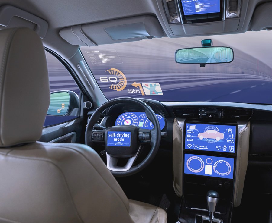
Automotive
Core Technology
Research and Development
Production Engineering
Simulation/ Evaluation & Analysis Technology
To Our Shareholders
IR Library
Message from the President
Sustainability Management
Sustainability Report
Initiatives for SDGs
RBA Code of Conduct Initiative
Initiatives for Environmental Issues
Initiatives for Social Issues
Governance
News
Topics (Renewal Information)
Corporate Outline
Global Network
Our Business
Our History
To Understand SHINKO
SHINKO at a Glance
The Shinko Group Mission, Vision, and Values
Code of Conduct
Related Information
Procurement