IC Assembly

Copper Pillar Bumping

Introduction

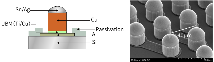
Copper pillars are terminals used to “flip-chip” IC chips to a substrate in a semiconductor package by TCFC (Thermal Compression Flip-Chip) technology. Copper pillars are formed on aluminum electrode pads of an IC chip. Copper pillar interconnects are seeing higher demand due to an increase in pin count with fine pad pitches integrated on an IC chip.
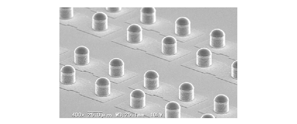
Copper pillars with dimensional uniformity can be formed on a silicon wafer by using fine plating pattern forming technology.

Features

  • Available wafer size: 12 inches (300 mm)
  • Clean process provided by fluxless reflow technology
  • Low-alpha-ray Sn-Ag solder plating is supported
  • Success of mass production on 40 μm IC pad pitches
  • Various bump shapes are available.
  • Fully equipped with automatic inspection system
  • Consistent assembly processes from Copper pillar formation to BGA/LGA semiconductor package assembly

Structure

Cuピラー.png

Application

  • Copper pillar formation on multi-pin IC chip
  • Fine pitch and micro-Copper pillar formation
  • Ultra-micro Copper pillar formation for research and development (Example : 10 μm diameter / 20 μm pitch)